Trial Dicing Experiment
The optimization of wafer dicing process involves the precise control of many variables directly and indirectly affected by Hardness, brittleness and thickness.
With new wafer materials such as gallium arsenide, lithium tantalum, and even copper joining the ranks of standard silicon, semiconductor manufacturers are facing new and greater challenges in maintaining and improving dicing productivity.
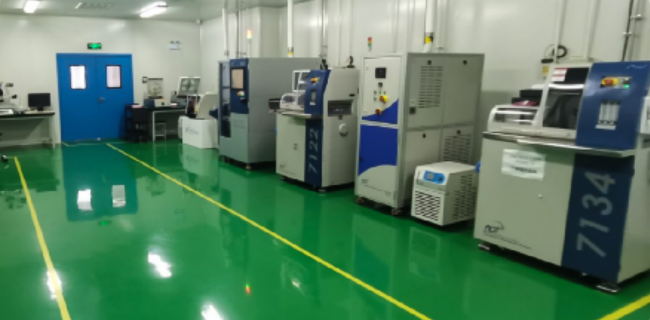
ADT continues to grow in the dicing equipment and blades used in semiconductor and electronic products, accumulating rich dicing experience.
At ADT, we continuously develop methods to quantify and adjust dicing blade materials and characteristics to improve and increase dicing quality, blade life, and production.
Technology driven development has become the gene of enterprises, with R&D investment exceeding 10% for consecutive years. The domestic team that adheres to the concept of " living in innovation " has successfully achieved localized R&D, and the performance of semiconductor dicing equipment is aligned with the industry benchmark.
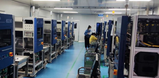
ADT has a wide range of research and development capabilities, including highly skilled personnel and well-equipped process development centers, where our engineers identify platforms, dicing blades, and dicing methods that are most suitable for solving specific challenges and general industry problems.

